
- PCB Fab
- Etching
- Exposure Machine
- Drilling Machine-Schmoll
- PTH Line
- Solderability Preservative
- Automatic Lamination
- Roll To Roll
- Inner Brown Oxide Line
- CNC Routing Machine
- Laser Direct Imaging
- Immersion Line
- Pre-Treatment
- PCB Assembly
- Automatic Loader
- Screen Printer
- High Speed Chips Mounter
- Multifunction IC Mounter
- Reflow
- Automatic Unloader
- BGA Rework Machine
- Electron Microscope
- Bake Oven
- Oven Temperature Tester
- Components
- Resistance
- Capacitance
- Inductance
- MOS
- MCU/ICS
- DC/DC
- Relays
- Module
- Others
- PCB Design
- AOI
- AOI Inspection
- X-Ray
- X-Ray
- Wave Soldering
- Wave Soldering
- ICT
- ICT
- Anti-Corrosion Paint
- Anti-Corrosion Paint
- Fixture Custom
- Fixture Custom
- LCD Screen Custormization
- LCD Screen Custormization


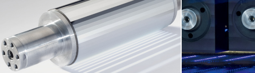
LASER DIRECT
IMAGING
288 laser beams, very robust beam guidance, and beam quality with low diffraction
WORKING PRINCIPLE The Laser Direct Imaging System SpeedLight 2D is used to expose the conductive pattern on a photoresist-coated panel, making the production and use of a traditional photo tool unnecessary.
 |
|
| Polygon Mirror with 48 Facets | Polygon Module During Exposure |
TECHNICAL SPECIFICATION
• Panel Size: up to 660 mm (W) × 650 mm (L) (extensible)
• Panel thickness: 0.05 mm to 8 mm
• Exposure field: up to 650 mm
• Throughput: 180 panels/hour (double-sided exposed)
FEATURES
High throughput due to twin stage system with up to 8,000 exposures per day
High volume and high resolutions at the same time
• Parallel data processing and data transmission for two panels
• Optical system with multi beam laser diodes and scanning polygons
• 288 laser diodes for powerful light source and high-speed exposure
• High throughput (panel/day) and low consumption costs, especially in case of small jobs
• Up to 8,000 exposures per day (22 hrs, 15 µm resolution on 660 × 650 mm format)
• Area of operation twice as big as competitive systems
• Throughput and performance is not limited by the typical bottlenecks of other digital imaging devices (e. g. solid-state laser, micromirror) Precise laser processing and handling
• Laser diodes with 500 MHz enabling 1.5 µm data grid
• Side-to-side positioning accuracy ± 10 µm Flexibility to technology and jobs
• “All-in-one” solution for different applications
• Fast change of job data
• Adaption to customers’ roadmaps
• Capable for both photoresist and soldermask Cost reduction
• No expenses for films and pilot exposures
• Low consumption costs
• Quick amortization compared to traditional film exposure


